In the manufacturing of Printed Circuit Board, through hole plating remains a complex operation. It involves wet chemical processes including deposition of metals by metallization and electroplating techniques. Although direct metallization has contributed to reduce the number of steps and chemicals involved in the process, it is still the source of a lot of anguish among the engineering community.
Printed Electronics is emerging as the technology that will replace traditional subtractive PCB manufacturing. With no wet chemistry it is widely considered a “green process” and falls in the category of additive technology.
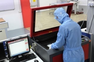
As a South East Asian leader of Printed Electronics, Central Midori pioneered in the development of a proprietary through-hole printing process using conventional screen-printing technique and silver conductive ink.
Substrate is generally made of polyester or polycarbonate film with thickness comprised between 50 and 125 microns – thinner is possible but generally requires heat stabilization first.
- The process begins with the printing of the top circuitry layer with Ag ink.
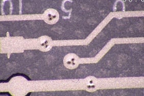
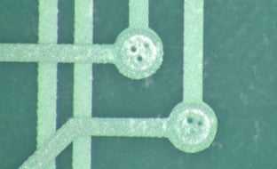
- Holes are then produced using laser drilling or hard tooling. Hole diameters do not exceed 0.3mm and are created in clusters of
- The printing of the bottom pad layer which fill up the holes with silver is the most challenging operation. All process parameters have to be carefully controlled in order to ensure the integrity of the printed through-hole.
Among them, the most important are:- 70 shore squeegee
- 3 to 5mm off-contact
- around 225 polyester mesh count (threads per inch)
- 12 micron emulsion
- “Chamfer” squeegee profile.
The viscosity of the ink is also critical and will be addressed in a separate blog post.
- A final Ag print pass on the top layer will finish to seal the hole.
The conventional way of producing a printed multilayer circuit is by alternating conductive and dielectric layers. Interlayer electrical connections are creating by leaving gaps in the dielectric pattern. Several pitfalls come from such “stack up constructions” including poor flexibility and risk of silver migration.
Through-hole printing is coming very handy to engineers to design the high density silver printed circuits of the future.
CMI has recently redesigned a stack-up construction into a double sided printed through-hole circuit and managed to solve our customer bending conundrum and at the same time improved our internal yield, killing 2 birds with one stone!